NorFlash is a common non-volatile storage medium, often used to store program firmware or some data, with the 25Qxx series in SOP-8 package as a representative.
The conventional way is to read and write byte by byte, which is not very cost-effective for interfaces like SPI.
When multiple bytes need to be read or written, DMA can be used to take over, saving a lot of CPU time.
Taking W25Q64 as an example, this article introduces how to use SPI with DMA to achieve flash read and write. The method is similar for NOR FLASH chips of other capacities or brands.The complete SPI requires four signals, connected to SPI2 here, CS can use any IO port, the connection between Flash and MCU is as follows:
CS – PB12
CLK – PB13 (SPI2_SCK)
DO – PB14 (SPI2_MISO)
DI – PB15 (SPI2_MOSI)


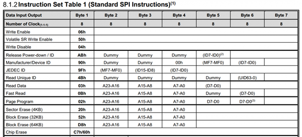
There are many instructions for Nor Flash, but only a few are commonly used.
The instructions that need to be implemented with DMA here are “Read Data” and “Page Program”, while other instructions are implemented in the traditional way.
Read Data 03h
Page Program 02h

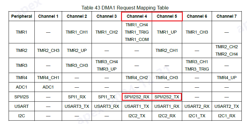
By consulting the DMA chapter of APM32E103xCxE User Manual, the corresponding channels for SPI2 are DMA1_Channel4 for SPI2 receive and DMA1_Channel5 for SPI2 transmit.

DMA1_Channel4 can be used for transferring read data from Flash, while DMA1_Channel5 can be used for transferring page programming of Flash.
Reference SDK initializes SPI as master, full-duplex mode is simple, the code is as follows.
void spi_flash_init(void)
{
GPIO_Config_T gpioConfig;
SPI_Config_T spiConfig;
/* Enable related Clock */
RCM_EnableAPB1PeriphClock(RCM_APB1_PERIPH_SPI2);
RCM_EnableAPB2PeriphClock(RCM_APB2_PERIPH_GPIOB);
/* config MISO*/
gpioConfig.pin = GPIO_PIN_14 ;
gpioConfig.mode = GPIO_MODE_AF_PP;
gpioConfig.speed = GPIO_SPEED_50MHz;
GPIO_Config(GPIOB, &gpioConfig);
/** config SCK,MOSI*/
gpioConfig.pin = GPIO_PIN_13 | GPIO_PIN_15;
gpioConfig.mode = GPIO_MODE_AF_PP;
gpioConfig.speed = GPIO_SPEED_50MHz;
GPIO_Config(GPIOB, &gpioConfig);
/** config CS */
gpioConfig.pin = GPIO_PIN_12;
gpioConfig.mode = GPIO_MODE_OUT_PP;
gpioConfig.speed = GPIO_SPEED_50MHz;
GPIO_Config(GPIOB, &gpioConfig);
GPIO_SetBit(GPIOB, GPIO_PIN_12);
GPIO_SetBit(GPIOB, GPIO_PIN_13);
GPIO_SetBit(GPIOB, GPIO_PIN_14);
GPIO_SetBit(GPIOB, GPIO_PIN_15);
SPI_ConfigStructInit(&spiConfig);
spiConfig.length = SPI_DATA_LENGTH_8B;
spiConfig.baudrateDiv = SPI_BAUDRATE_DIV_64;
/* 2 line full duplex */
spiConfig.direction = SPI_DIRECTION_2LINES_FULLDUPLEX;
/* LSB first */
spiConfig.firstBit = SPI_FIRSTBIT_MSB;
/* Slave mode */
spiConfig.mode = SPI_MODE_MASTER;
/* Polarity is low */
spiConfig.polarity = SPI_CLKPOL_HIGH;
/* Software select slave enable */
spiConfig.nss = SPI_NSS_SOFT;
/* Phase is 1 edge */
spiConfig.phase = SPI_CLKPHA_2EDGE;
spiConfig.crcPolynomial = 7;
/* SPI config */
SPI_Config(SPI2, &spiConfig);
SPI_ConfigDataSize(SPI2, SPI_DATA_LENGTH_8B);
SPI_Enable(SPI2);
}
To achieve DMA read and write, it is necessary to configure two DMA channels. The configuration of the two DMA channels is slightly different, mainly focusing on the direction of transfer.
DMA1_Channel5 is used for transmission, with the direction from memory to peripheral;
DMA1_Channel4 is used for reception, with the direction from peripheral to memory.
The address of the peripheral is the SPI data register address, which can be found in the manual as SPI2_BASE + 0×0C.
The memory address and transfer length can be left unconfigured for now, and both DMA channels should not be enabled until actual transmission is required later.
DMA_Config_T DMA_ConfigStruct;
void spi_fullduplex_dma_init(void)
{
RCM_EnableAHBPeriphClock(RCM_AHB_PERIPH_DMA1);
DMA_ConfigStruct.peripheralBaseAddr = (uint32_t)(SPI2_BASE + 0x0C) ;
DMA_ConfigStruct.peripheralInc = DMA_PERIPHERAL_INC_DISABLE;
DMA_ConfigStruct.memoryInc = DMA_MEMORY_INC_ENABLE;
DMA_ConfigStruct.peripheralDataSize = DMA_PERIPHERAL_DATA_SIZE_BYTE;
DMA_ConfigStruct.memoryDataSize = DMA_MEMORY_DATA_SIZE_BYTE;
DMA_ConfigStruct.loopMode = DMA_MODE_NORMAL;
DMA_ConfigStruct.priority = DMA_PRIORITY_HIGH;
DMA_ConfigStruct.M2M = DMA_M2MEN_DISABLE;
//SPI2_TX DMA_CH5
DMA_Reset(DMA1_Channel5);
DMA_ConfigStruct.memoryBaseAddr = (uint32_t) AddressBuffer;
DMA_ConfigStruct.dir = DMA_DIR_PERIPHERAL_DST;
DMA_ConfigStruct.bufferSize = 0;
DMA_Config(DMA1_Channel5, &DMA_ConfigStruct);
SPI_I2S_EnableDMA(SPI2, SPI_I2S_DMA_REQ_TX);
//SPI2_RX DMA_CH4
DMA_Reset(DMA1_Channel4);
DMA_ConfigStruct.memoryBaseAddr = (uint32_t) AddressBuffer;
DMA_ConfigStruct.dir = DMA_DIR_PERIPHERAL_SRC;
DMA_ConfigStruct.bufferSize = 0;
DMA_Config(DMA1_Channel4, &DMA_ConfigStruct);
SPI_I2S_EnableDMA(SPI2, SPI_I2S_DMA_REQ_RX);
}
When sending multiple data, set the DMA1_Channel5 memory address, transmission length, enable memory address incrementation, and then enable DMA transfer; DMA1_Channel4 is similar, except the address does not need to increment. Finally, wait for the transfer to complete to achieve SPI DMA transmission.
If a large amount of data is being sent, the waiting time may be long. During the waiting process, the CPU can perform other tasks.
void spi_dam_transmit_buffer(unsigned char *buffer, unsigned int length)
{
DMA1_Channel4->CHCFG_B.MIMODE = DISABLE;
DMA1_Channel4->CHMADDR = (uint32_t)AddressBuffer;
DMA1_Channel4->CHNDATA = length;
DMA1_Channel5->CHCFG_B.MIMODE = ENABLE ;
DMA1_Channel5->CHMADDR = (uint32_t)buffer;
DMA1_Channel5->CHNDATA = length;
DMA1_Channel4->CHCFG_B.CHEN = ENABLE;
DMA1_Channel5->CHCFG_B.CHEN = ENABLE;
while (DMA_ReadStatusFlag(DMA1_FLAG_TC5) == RESET);
DMA_ClearStatusFlag(DMA1_FLAG_TC5);
while (DMA_ReadStatusFlag(DMA1_FLAG_TC4) == RESET);
DMA_ClearStatusFlag(DMA1_FLAG_TC4);
DMA1_Channel5->CHCFG_B.CHEN = DISABLE;
DMA1_Channel4->CHCFG_B.CHEN = DISABLE;
}
When receiving multiple data, besides setting DMA1_Channel4, DMA1_Channel5 also needs to be set. Because the MCU acts as the host to provide clock for the flash chip, the sending should be opened while reading.
For the sending part, any data can be sent, so the memory address of the sending channel does not need to be incremented, just assign it to a custom small array.
Regarding the receiving part, similar to the previous, set the memory address, send length, enable memory address auto-increment, enable the transfer of DMA1_Channel4, and wait for both channels to finish transferring to complete the reading.
void spi_dam_receive_buffer(unsigned char *buffer, unsigned int length)
{
DMA1_Channel5->CHCFG_B.MIMODE = DISABLE;
DMA1_Channel5->CHMADDR = (uint32_t)AddressBuffer;
DMA1_Channel5->CHNDATA = length;
DMA1_Channel4->CHCFG_B.MIMODE = ENABLE ;
DMA1_Channel4->CHMADDR = (uint32_t)buffer;
DMA1_Channel4->CHNDATA = length;
DMA1_Channel4->CHCFG_B.CHEN = ENABLE;
DMA1_Channel5->CHCFG_B.CHEN = ENABLE;
while (DMA_ReadStatusFlag(DMA1_FLAG_TC5) == RESET);
DMA_ClearStatusFlag(DMA1_FLAG_TC5);
while (DMA_ReadStatusFlag(DMA1_FLAG_TC4) == RESET);
DMA_ClearStatusFlag(DMA1_FLAG_TC4);
DMA1_Channel5->CHCFG_B.CHEN = DISABLE;
DMA1_Channel4->CHCFG_B.CHEN = DISABLE;
}
The driver code for NorFlash is mostly the same as the regular SPI method, just needing modifications to the code regarding these two instructions:
NorFlash data read
The process of reading multiple data is similar to the method without using DMA, except that the part where data is read using a for loop is replaced with spi_dma_receive_buffer().
void w25qxxx_read(unsigned char *buf, unsigned int addr, unsigned short num)
{
unsigned short i;
w25qxxx_cs_set(0); // Enable device
w25qxxx_wr_byte(W25XXX_ReadData); // Send read command
w25qxxx_wr_byte((unsigned char)((addr) >> 16)); // Send 24-bit address
w25qxxx_wr_byte((unsigned char)((addr) >> 8));
w25qxxx_wr_byte((unsigned char)addr);
spi_dam_receive_buffer(buf, num);
w25qxxx_cs_set(1);
}
void w25qxxx_write_page(unsigned char *buf, unsigned int addr, unsigned short num)
{
unsigned short i;
w25qxxx_write_enable(); // SET WEL
w25qxxx_cs_set(0); // Enable
w25qxxx_wr_byte(W25XXX_PageProgram); // Send write page command
w25qxxx_wr_byte((unsigned char)((addr) >> 16)); // Send 24-bit address
w25qxxx_wr_byte((unsigned char)((addr) >> 8));
w25qxxx_wr_byte((unsigned char)addr);
spi_dam_transmit_buffer(buf, num);
w25qxxx_cs_set(1); // Deselect chip
w25qxxx_wait_busy(); // Wait for write to finish
}
Finally, we validate whether the above code is feasible, first initialize the SPI and corresponding DMA.
//Initialization
void w25qxxx_init()
{
spi_flash_init();
spi_fullduplex_dma_init();
}
Then read the ID of the chip, this step is mainly to confirm if the hardware is normal.
FlashChipID = w25qxxx_read_id();
Next, write data from 0×00-0xFF to any sector, erase the sector, write to the sector again, read the data from the sector, and compare the read data with the original data written.
//Flash test
unsigned short FlashChipID;
unsigned char flash_test_write_buffer[4096];
unsigned char flash_test_read_buffer[4096];
unsigned int AddrSector=0;
void w25qxxx_test()
{
unsigned int i;
for(i=0;i<4096;i++)
{
flash_test_write_buffer[i]=i%256;
}
w25qxxx_erase_sector(AddrSector);
w25qxxx_write_sector(flash_test_write_buffer,AddrSector);
w25qxxx_read(flash_test_read_buffer,AddrSector*4096,4096);
if(memcmp(flash_test_read_buffer,flash_test_write_buffer,4096)==0)
{
printf("flash write success.");
}
else
{
printf("flash write failed!");
}
}
