Remapping PD0 (OSC_IN) and PD1 (OSC_OUT) to GPIO on APM32F103/E103
Recently, I received an urgent question regarding the APM32F103/E103 chips:
“Please tell me how to set up PD0 (osc_in) and PD1 (osc_out) as GPIO.
I’m in a hurry so please let me know early.
GPIO_ConfigPinRemap(GPIO_REMAP_PD01);
gpioConfig.pin = GPIO_PIN_0 | GPIO_PIN_1;
gpioConfig.mode = GPIO_MODE_IN_FLOATING;
GPIO_Config(GPIOD, &gpioConfig);
GPIOD->ODATA |= (GPIO_PIN_0 | GPIO_PIN_1);
Such a requirement is actually very common, especially on small-package MCUs with limited pin resources. Today, let’s explore—based on the official Geehy datasheet—how to remap PD0 (OSC_IN) and PD1 (OSC_OUT) to general-purpose I/O, and uncover the powerful features of the AFIO peripheral.
1. What the Datasheet Says
By consulting the APM32F103/E103 datasheet, you’ll find that on smaller packages (e.g. QFN36, LQFP48, LQFP64), pins PD0 and PD1 default to the external crystal oscillator function (OSC_IN/OSC_OUT), but they also support GPIO remapping.
The original Geehy statement reads:
For Pin 2 and Pin 3 of QFN36 package, and Pin 5 and Pin 6 of LQFP48 and LQFP64 package, the default configuration after reset is OSC_IN and OSC_OUT. Software can remap these two pins to PD0 and PD1 functions; for LQFP100 package, PD0 and PD1 are inherent function pins. This multiplexing can be configured in software (if the package model supports these pins). See the “Multiplexing Function I/O” and “Debugging Setting” sections of the user manual for details.
In short: on small packages, OSC is the reset default, but you can remap them to ordinary GPIO via AFIO.
2. Relevant Manual Chapters
The detailed AFIO and pin-multiplexing descriptions live in Chapter 12: Alternate Function Input/Output Pin (AFIO).
In package products with less than 100 pins, the user can set AFIO_REMAP1/2 (multiplexing remapping and debug I/O configuration register) to realize the remapping of general I/O PD0/PD1 to external oscillator pin OSC_IN/OSC_OUT. Then PD0 and PD1 cannot be used to generate external interrupt time.

These features make the MCU’s I/O far more flexible and powerful.
3. Key Points for AFIO Configuration
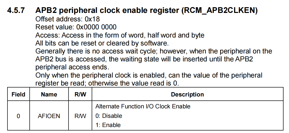
AFIO is an independent peripheral on the APB2 bus. To use its remap features, you must enable the AFIO clock on APB2 first—otherwise your remap calls will have no effect.
Merely configuring GPIO without AFIO remapping will not change the pin functions.
Typical setup flow:
Enable the AFIO clock

Call the remap function
Configure GPIO mode
4. Packaging & Special Notes
- LQFP100 packages have another pair of PD0/PD1 (pins 81, 82). You can also remap these via AFIO to OSC_IN/OSC_OUT in software.
- For different packages, the availability and pin numbers of PD0/PD1 vary—always refer to the datasheet’s pin-assignment and AFIO chapters.
5. Extended Value of AFIO
Beyond turning unused oscillator pins into GPIO, AFIO offers:
- Flexible switching between debug and normal pin functions
- Dynamic assignment of interrupt lines
- Increased pin-multiplexing, saving PCB/BOM cost
6. CAN-Function Considerations
Important: If your application requires using the CAN bus, note that CAN demands high clock accuracy.
We strongly advise against using CAN when there is no external crystal (i.e. when you’ve remapped OSC_IN/OSC_OUT to GPIO), especially if PD0/PD1 serve as CAN_TX/CAN_RX. Otherwise, CAN communication may become unstable or fail altogether.
Conclusion
To remap APM32’s OSC_IN/OSC_OUT to GPIO:
- Enable the AFIO clock
- Call the appropriate remap function
- Perform standard GPIO configuration
And please notice:
- If you need CAN, always keep the external crystal oscillator intact—don’t turn those pins into GPIO.