This article details a dual ADC synchronous sampling solution using the APM32F402 series MCU, which achieves high-precision, simultaneous acquisition of three analog signals through the injected channel mechanism.
I. System Design
- Achieve synchronous triggering of ADC1 and ADC2 to eliminate sampling time differences between channels.
- Utilize the high-priority feature of injected channels to ensure preferential processing of critical signals.
- Configure the timer trigger source for precise sampling period control.
- Optimize the interrupt handling process to enhance the system’s real-time response capability.
II. Hardware Architecture Details
2.1 Core Chip Selection
This design selects the APM32F402 series MCU from Geehy Semiconductor, which features the following key characteristics:
- Dual ADC modules supporting synchronous sampling mode.
- System main frequency up to 120MHz, providing powerful processing capabilities.
- Rich timer resources supporting various trigger modes.
- 12-bit ADC resolution with a sampling rate of up to 1MHz.
2.2 Pin Allocation and Signal Connection
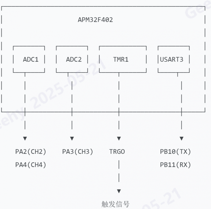
Analog Input Section:
- PA2 (ADC1_CH2): Connected to the 1st analog signal source.
- PA3 (ADC2_CH3): Connected to the 2nd analog signal source.
- PA4 (ADC2_CH4): Connected to the 3rd analog signal source.
Trigger Control Section:
- TMR1_TRGO: Trigger output from Timer 1, connected to the ADC trigger input.
Communication Interface Section:
- PB10 (USART3_TX): Serial port transmit, used for outputting debug information.
- PB11 (USART3_RX): Serial port receive, can be extended for receiving commands from a host computer.
III. Software Implementation Details
3.1 Dual ADC Synchronous Sampling Configuration
The core of the software design is to configure the dual ADCs in a synchronous working mode to achieve simultaneous acquisition of the three signals. The key code is as follows:
void ADC_Init(void)
{
// 1. Enable GPIO and ADC clocks
RCM_EnableAPB2PeriphClock(RCM_APB2_PERIPH_GPIOA);
RCM_EnableAPB2PeriphClock(RCM_APB2_PERIPH_ADC1 | RCM_APB2_PERIPH_ADC2);
// 2. Configure analog input pins
GPIO_Config_T GPIO_ConfigStruct;
GPIO_ConfigStructInit(&GPIO_ConfigStruct);
GPIO_ConfigStruct.mode = GPIO_MODE_ANALOG;
GPIO_ConfigStruct.pin = GPIO_PIN_2 | GPIO_PIN_3 | GPIO_PIN_4;
GPIO_Config(GPIOA, &GPIO_ConfigStruct);
// 3. Configure ADC1
ADC_Config_T ADC_ConfigStruct;
ADC_Reset(ADC1);
ADC_ConfigStructInit(&ADC_ConfigStruct);
ADC_ConfigStruct.mode = [color=blue]ADC_MODE_INJEC_SIMULT[/color]; // Injected simultaneous mode
ADC_ConfigStruct.scanConvMode = ENABLE; // Scan conversion mode
ADC_ConfigStruct.continuousConvMode = DISABLE; // Single conversion mode
ADC_ConfigStruct.externalTrigConv = ADC_EXT_TRIG_CONV_NONE;
ADC_ConfigStruct.dataAlign = ADC_DATA_ALIGN_RIGHT;
ADC_ConfigStruct.nbrOfChannel = 3;
RCM_ConfigADCCLK(RCM_PCLK2_DIV_6); // ADCCLK = 120MHz/6 = 20MHz
// 4. Configure ADC1 injected channel
ADC_ConfigInjectedSequencerLength(ADC1, 1);
ADC_ConfigInjectedChannel(ADC1, ADC_CHANNEL_2, 1, ADC_SAMPLETIME_13CYCLES5);
ADC_ConfigExternalTrigInjectedConv(ADC1, ADC_EXT_TRIG_INJEC_CONV_TMR1_TRGO);
// 5. Configure ADC2 injected channels
ADC_Reset(ADC2);
ADC_Config(ADC2, &ADC_ConfigStruct);
ADC_ConfigInjectedSequencerLength(ADC2, 2);
ADC_ConfigInjectedChannel(ADC2, ADC_CHANNEL_3, 1, ADC_SAMPLETIME_13CYCLES5);
ADC_ConfigInjectedChannel(ADC2, ADC_CHANNEL_4, 2, ADC_SAMPLETIME_13CYCLES5);
ADC_ConfigExternalTrigInjectedConv(ADC2, ADC_EXT_TRIG_INJEC_CONV_TMR1_TRGO);
// 6. Enable interrupt and start ADC
ADC_EnableInterrupt(ADC1, ADC_INT_INJEOC);
ADC_EnableInterrupt(ADC2, ADC_INT_INJEOC);
NVIC_EnableIRQRequest(ADC1_2_IRQn, 0, 0);
// 7. ADC calibration and startup
ADC_Enable(ADC1);
ADC_ResetCalibration(ADC1);
while (ADC_ReadResetCalibrationStatus(ADC1));
ADC_StartCalibration(ADC1);
while (ADC_ReadCalibrationStartFlag(ADC1));
ADC_Enable(ADC2);
ADC_ResetCalibration(ADC2);
while (ADC_ReadResetCalibrationStatus(ADC2));
ADC_StartCalibration(ADC2);
while (ADC_ReadCalibrationStartFlag(ADC2));
// 8. Start injected conversion
ADC_EnableSoftwareStartInjectedConv(ADC1);
ADC_EnableSoftwareStartInjectedConv(ADC2);
}
3.2 Timer Trigger Configuration
Timer TMR1 is configured in center-aligned mode to generate a periodic trigger signal:
void TMR_Init(void)
{
// 1. Enable timer and GPIO clocks
RCM_EnableAPB2PeriphClock(RCM_APB2_PERIPH_TMR1);
RCM_EnableAPB2PeriphClock(RCM_APB2_PERIPH_GPIOA | RCM_APB2_PERIPH_GPIOB);
// 2. Configure PWM output pins (can be used for applications like motor control)
GPIO_Config_T gpioConfig;
gpioConfig.speed = GPIO_SPEED_50MHz;
gpioConfig.mode = GPIO_MODE_AF_PP;
gpioConfig.pin = GPIO_PIN_8 | GPIO_PIN_9 | GPIO_PIN_10; // PWM output pins
GPIO_Config(GPIOA, &gpioConfig);
// 3. Configure basic timer parameters
TMR_BaseConfig_T tmrBaseConfig;
tmrBaseConfig.countMode = [color=blue]TMR_COUNTER_MODE_CENTERALIGNED1[/color]; // Center-aligned mode 1
tmrBaseConfig.clockDivision = TMR_CLOCK_DIV_1;
tmrBaseConfig.period = 999; // Period value
tmrBaseConfig.division = 11999; // Prescaler value
tmrBaseConfig.repetitionCounter = 1; // Repetition counter
TMR_ConfigTimeBase(TMR1, &tmrBaseConfig);
// 4. Configure PWM output mode (example)
TMR_OCConfig_T tmrOCConfig;
tmrOCConfig.mode = TMR_OC_MODE_PWM2;
tmrOCConfig.outputState = TMR_OC_STATE_ENABLE;
tmrOCConfig.outputNState = TMR_OC_NSTATE_ENABLE;
tmrOCConfig.pulse = 500; // 50% duty cycle
TMR_ConfigOC1(TMR1, &tmrOCConfig);
TMR_ConfigOC2(TMR1, &tmrOCConfig);
TMR_ConfigOC3(TMR1, &tmrOCConfig);
// 5. Configure trigger output (key step)
TMR_SelectOutputTrigger(TMR1, TMR_TRGO_SOURCE_UPDATE); // Use update event as trigger source
// 6. Configure dead-time (for complementary PWM output)
TMR_BDTConfig_T TIM_BDTRStruct;
TIM_BDTRStruct.deadTime = 0x1D; // Approx. 2μs dead-time
TIM_BDTRStruct.BRKState = TMR_BRK_STATE_DISABLE;
TMR_ConfigBDT(TMR1, &TIM_BDTRStruct);
// 7. Enable timer and PWM outputs
TMR_EnablePWMOutputs(TMR1);
TMR_Enable(TMR1);
}
3.3 Interrupt Handling Mechanism
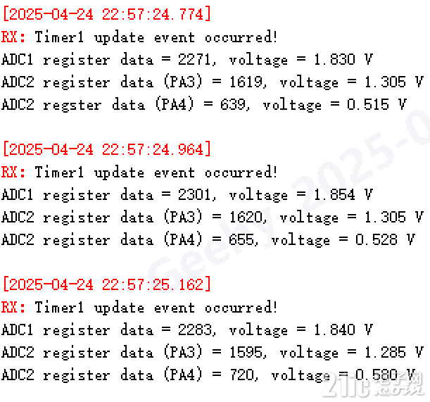
After the ADC conversion is complete, an interrupt is triggered. The sampled values are read and processed in the interrupt service routine:
void ADC1_2_IRQHandler(void)
{
// 1. Mark entry into interrupt (for debugging)
GPIO_SetBit(GPIOC, GPIO_PIN_13);
// 2. Handle ADC1 injected channel conversion complete event
if (ADC_ReadIntFlag(ADC1, ADC_INT_INJEOC) == SET)
{
uint16_t adc1_value = ADC_ReadInjectedConversionValue(ADC1, ADC_INJEC_CHANNEL_1);
float voltage = (float)adc1_value / 4095 * 3.3; // Convert to voltage value
printf("ADC1 (PA2) Data: %d, Voltage: %.3f V\r\n", adc1_value, voltage);
ADC_ClearIntFlag(ADC1, ADC_INT_INJEOC); // Clear interrupt flag
}
// 3. Handle ADC2 injected channel conversion complete event
if (ADC_ReadIntFlag(ADC2, ADC_INT_INJEOC) == SET)
{
uint16_t adc2_ch3 = ADC_ReadInjectedConversionValue(ADC2, ADC_INJEC_CHANNEL_1);
uint16_t adc2_ch4 = ADC_ReadInjectedConversionValue(ADC2, ADC_INJEC_CHANNEL_2);
printf("ADC2 (PA3) Data: %d, Voltage: %.3f V\r\n", adc2_ch3, adc2_ch3*3.3/4095);
printf("ADC2 (PA4) Data: %d, Voltage: %.3f V\r\n", adc2_ch4, adc2_ch4*3.3/4095);
ADC_ClearIntFlag(ADC2, ADC_INT_INJEOC); // Clear interrupt flag
}
// 4. Mark completion of interrupt handling
GPIO_ResetBit(GPIOC, GPIO_PIN_13);
}
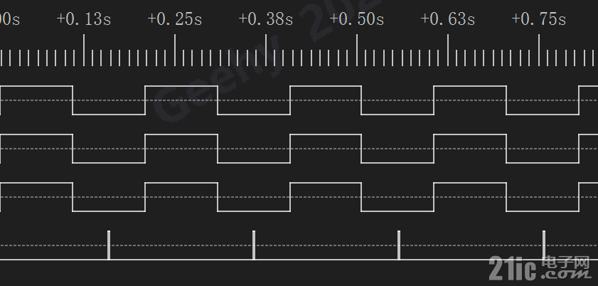
IV. Test Results
- Timer TMR1 counting frequency: 120MHz / (11999+1) = 10kHz
- Actual sampling frequency: 10kHz × 2 = 20kHz (due to center-aligned mode triggering on both up and down counting)
- Sampling time per ADC channel: 1 / 20kHz = 50μs