Does a programming failure always mean the FLASH is faulty?
Recently, an APM32 chip that failed programming was submitted from the production line (a rare occurrence, 1 in over 10,000 units in mass production). The symptom pointed to a FLASH failure, but the analysis revealed it was actually an SRAM failure. Here is the record of my analysis process:
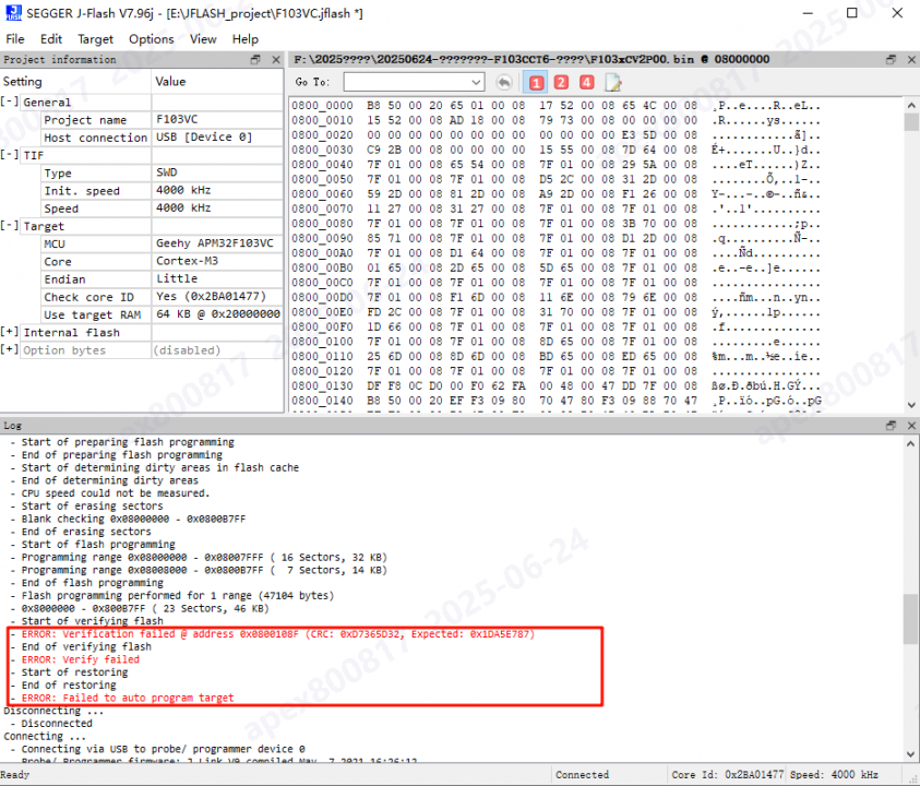
1) Programming Failure Phenomenon
- Test Method: Use J-Flash to program the .bin file and observe the phenomenon.
- Test Result: A verification error occurred during programming, and the FLASH address where the error occurred was reported.
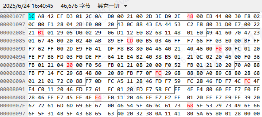
2) Comparing FLASH Content
- Test Method: When the anomaly occurred, read back the FLASH content and compare it with the original file.
- Test Result: Reading back the FLASH content and comparing it with the original file revealed that in some locations, FLASH data bits had flipped from 0 to 1, such as 48->4A, B1->B3, CD->CF, etc.
3) FLASH Read/Write Test
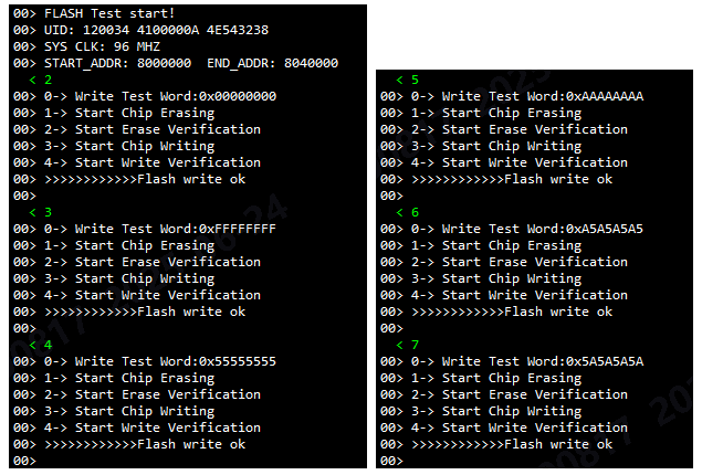
- Test Method: Run a full-chip erase, write, and read test on the FLASH from SRAM.
- Test Result: Multiple test patterns and different methods like chip erase/page erase were tried, and no abnormalities were found. The FLASH should be fine.
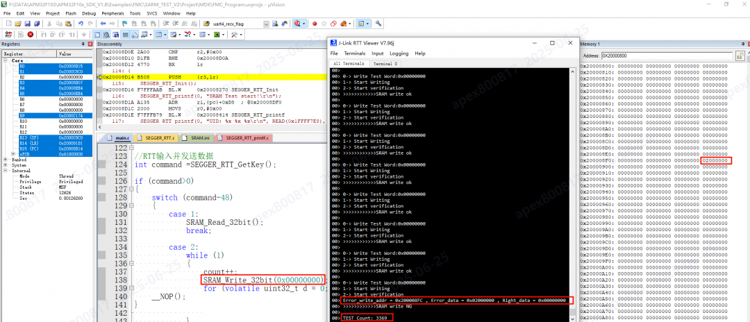
4) SRAM Read/Write Test
- Test Method: During J-Flash programming, data is moved into the FLASH by a loader program and a buffer located in SRAM. Therefore, with the FLASH test showing no issues, the next step is to test the SRAM.
- Test Result: An anomaly was found after 3369 cycles of testing the SRAM at a main clock frequency of 96MHz. Comparing the data confirmed that at SRAM address
5) Lowering Main Clock Frequency Test
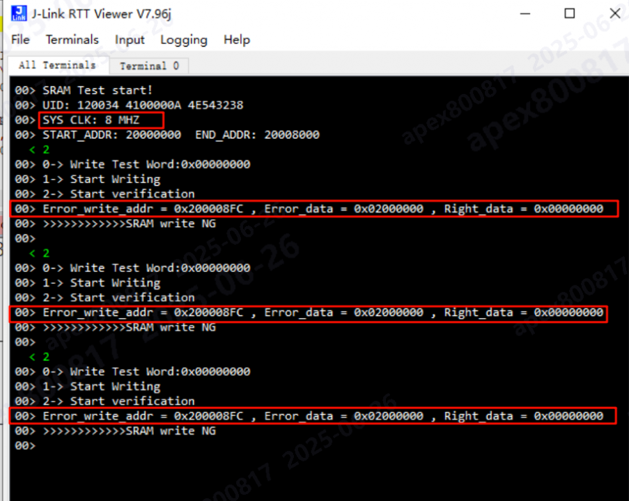
- Test Method: The probability of reproducing the anomaly was low at 96MHz. Considering that the actual programming of the .bin file is driven by an 8MHz clock, I tried lowering the main frequency for the SRAM test.
- Test Result: Using an 8MHz main clock, the SRAM anomaly at address 0×200008FF was detected on the very first test run. Possible Mechanism: An SRAM storage cell is similar to an RS flip-flop with two stable states. If there is leakage current during a read, a short read time might not be long enough to cause an erroneous flip. However, if the read is slower, the leakage current might cause the state to flip, leading to a read error.
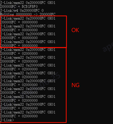
6) Failed Address Read/Write Test
- Test Method: Perform targeted read/write verification on the specific failing address.
- Test Result: After writing 0×00, the first few reads were normal (0×00). After several more reads, the data bit flipped, and the read value became abnormal (0×02).
7) Conclusion
The analysis confirmed that this programming failure was caused by an anomaly in the SRAM: the bit1 at address 0×200008FF was prone to a read error, flipping from 0 to 1. An SRAM anomaly can lead to both program execution errors and programming errors (since programming requires running a loader program and buffering FLASH data in SRAM).
**This programming failure case provides a deeper insight into the MCU’s programming mechanism. When a programming tool fails verification and reports an error address (usually in the FLASH area), the true point of failure could be the FLASH or it could be the SRAM; both need to be investigated.