1. What is QSPI XIP?
The main differences between QSPI (Quad SPI) and Standard SPI are:
- Speed: The data lines are upgraded from the original MOSI/MISO to four lines (IO0IO3), significantly boosting data transfer speeds.
- Management: The controller provides automatic management of instruction and address phases, as well as a memory-mapped mode, making it much more convenient to use.
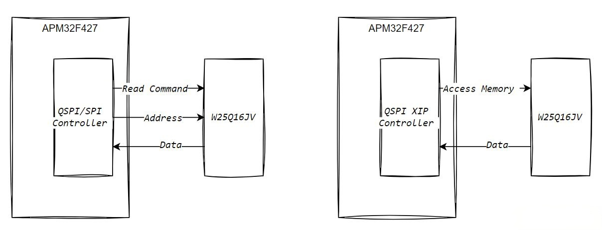
XIP (eXecute In Place) is the Key Feature of QSPI memory mapping.
- Traditional SPI: When reading/writing external Flash, software must send instructions and configure addresses every single time. It is cumbersome.
- QSPI + XIP: This maps the external Flash directly into the MCU’s address space, making reading data as simple as reading internal memory.
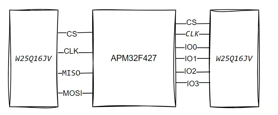
2. On-board W25Q16JV External Flash
The APM32F427 Tiny board is equipped with a W25Q16JV (16Mbit capacity), which supports various read instructions such as Quad I/O and Fast Read. By utilizing the correct instruction codes, address modes, and Dummy Cycles, high-speed access can be achieved. This aligns with our focus on high-performance MCU solutions.
3. Driver Flow for QSPI XIP Memory Mapping (Code Example)
The following section is sourced from the APM32F4xx_DAL_SDK_V1.3.0 sample project. It has been modified based on the “QSPI_ReadWrite” routine to demonstrate how to implement erasing, writing, and reading of the W25Q16JV, as well as how to enter XIP memory-mapped mode.
3.1 Basic Read/Write Operations
Before enabling XIP, we must first test the basic erase and write flow to ensure the communication path with the external Flash is functional. The steps are roughly as follows:
- Erase a specified sector.
- Write test data.
- Read back to verify.
- If the check passes, everything is ready.
Code Snippet:
/* Erase sector */
FLASH_EraseSector(0);
LOG_Print("FLASH_EraseSector (Sector 0 erased).\r\n");
LOG_Print("Data read from offset 0 via QSPI. Dump rxBuffer:\r\n");
FLASH_ReadData(0, rxBuffer, BUFFER_SIZE);
PrintArray32((uint32_t *)rxBuffer, BUFFER_SIZE / sizeof(uint32_t));
/* Write data */
FLASH_WriteData(0, txBuffer, BUFFER_SIZE);
LOG_Print("Data written to offset 0 via QSPI. Dump txBuffer:\r\n");
PrintArray32((uint32_t *)txBuffer, BUFFER_SIZE / sizeof(uint32_t));
/* Read data */
FLASH_ReadData(0, rxBuffer, BUFFER_SIZE);
LOG_Print("Data read from offset 0 via QSPI. Dump rxBuffer:\r\n");
PrintArray32((uint32_t *)rxBuffer, BUFFER_SIZE / sizeof(uint32_t));
/* Compare data */
if (BufferCmp((uint8_t*)txBuffer, (uint8_t*)rxBuffer, BUFFER_SIZE) != true)
{
BOARD_LED_On(LED3);
LOG_Print("Data compare failed! Error_Handler.\r\n");
Error_Handler();
}
LOG_Print("Data compare success!\r\n");
If the operations above complete smoothly, the erase and write process is fully functional.
3.2 One-Click Switch to XIP Mode
Once basic R/W is confirmed, we can enable XIP. You simply need to call a FLASH_EnterXIPMode() function in main.c. Its core utilizes the MemoryMapped feature of the QSPI controller:
void FLASH_EnterXIPMode(void)
{
QSPI_XIPTypeDef xipConfig = {0};
// 1) Instruction code: 0xEB (Quad I/O Fast Read)
xipConfig.Instruction = 0xEB;
// 2) WrapCode: if not using wrap, set 0
xipConfig.WrapCode = 0x00;
// 3) Address size: 24 bits, suitable for W25Q16JV
xipConfig.AddressSize = QSPI_XIP_ADDRESS_SIZE_24_BITS;
// 4) InstructionMode: how instruction and address are transmitted
// e.g. QSPI_XIP_INSTRUCTION_STANDARD_INS_ADDR, QSPI_XIP_INSTRUCTION_FRF_INS_ADDR
xipConfig.InstructionMode = QSPI_XIP_INSTRUCTION_STANDARD_INS;
// 5) Instruction bit length
xipConfig.InstructionSize = QSPI_XIP_INSTRUCTION_SIZE_8_BITS;
// 6) FrameFormat: QUAD
xipConfig.FrameFormat = QSPI_XIP_FRAME_FORMAT_QUAD;
// 7) DummyCycles: typically 6~10 cycles for 0xEB in W25Q16JV
xipConfig.DummyCycles = 6;
// 8) Endianness: little-endian
xipConfig.Endianness = QSPI_XIP_MEM_ACCESS_FORMAT_LITTLE_ENDIAN;
// 9) ContinuousMode / PrefetchMode
// For higher performance, can enable them if needed
xipConfig.ContinuousMode = ENABLE;
xipConfig.PrefetchMode = ENABLE;
// Enable chip select, then call the library function to enter memory-mapped mode
FLASH_ChipSelect(ENABLE);
if (DAL_QSPIEx_MemoryMapped(&hqspi, &xipConfig) != DAL_OK)
{
Error_Handler();
}
}
The configuration points in the code are primarily determined by the connected SPI Flash parameters:
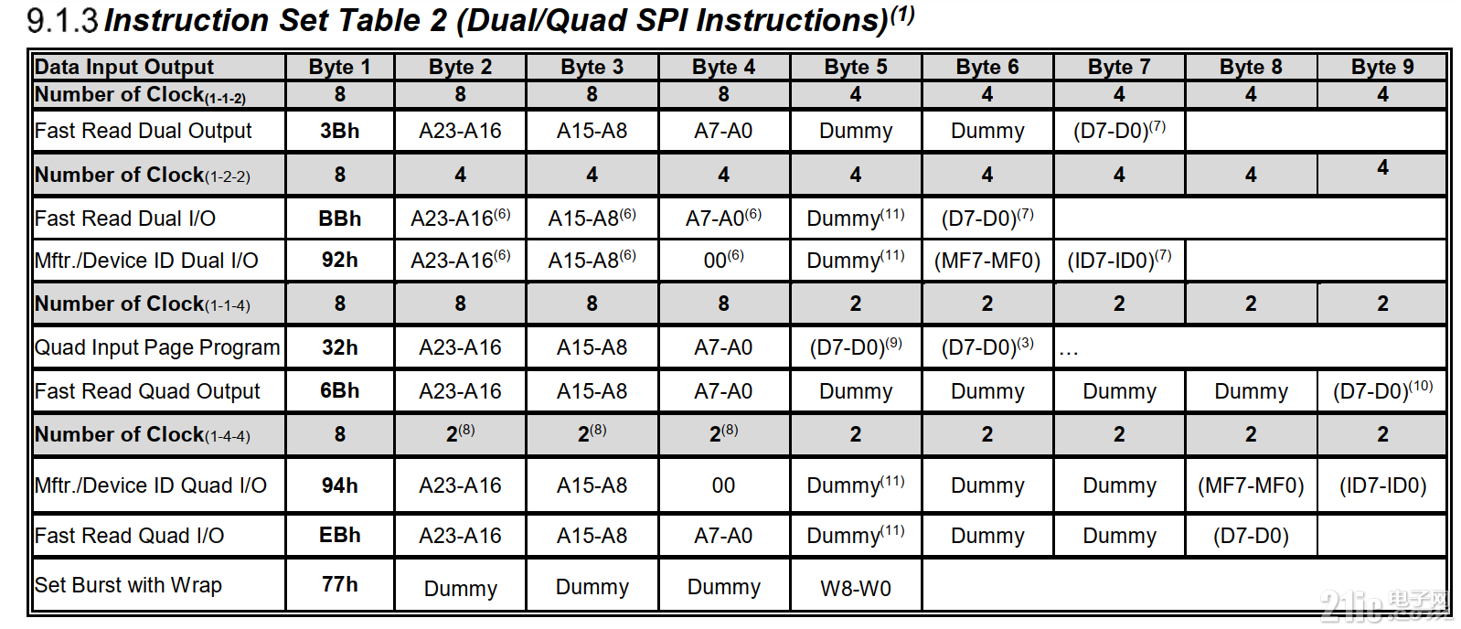
- Mode: Fast Read Quad I/O (0xEB)
- Address: 24-Bit
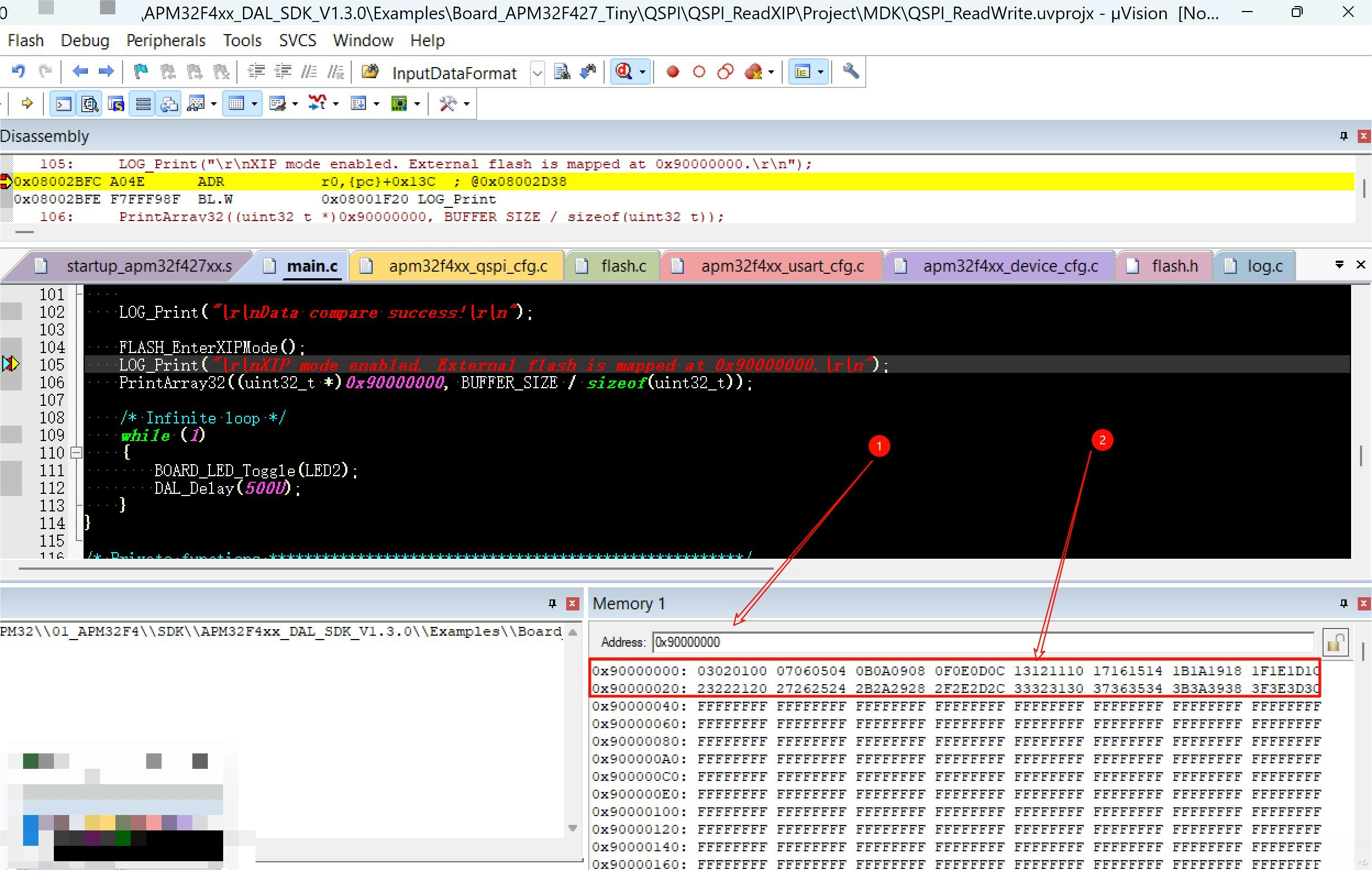
Once this function executes, the W25Q16JV is “mapped” to address 0×90000000. From then on, accessing this address automatically triggers the READ instruction + address + data return, without the need to write further instruction/address logic. You can verify it like this:
FLASH_EnterXIPMode();
LOG_Print("XIP mode enabled. External flash is mapped at 0x90000000.\r\n");
PrintArray32((uint32_t *)0x90000000, BUFFER_SIZE / sizeof(uint32_t));
As long as the printed data matches what was written previously, the XIP setup is successful!
4. How to Verify XIP Success Based on Experimental Phenomena
Serial Log: If read(0×90000000) matches the original written data perfectly, XIP is working properly.
Debugger Memory Window (e.g., MDK, IAR): Directly view the 0×90000000 region. Seeing the same content as in the Flash confirms a seamless integration.
Summary
The APM32F427 utilizes QSPI XIP to significantly enhance the external Flash user experience:
- Eliminates the hassle of frequently sending instructions and setting addresses.
- Provides fast continuous read speeds with simple code logic.
While XIP might not be essential for small data storage, it becomes a powerful asset for projects requiring code execution in place (Execute In Place) or rapid access to data exceeding internal capacity. This capability complements our high-performance MCU portfolio, similar to the APM32F411 series.
Attachment:
Here is the sample code: upload attachment:
Please place it in the APM32F4xx_DAL_SDK_V1.3.0\Examples\Board_APM32F427_Tiny\QSPI directory for use~