01. INTRODUCTION TO EMBEDDED MEMORY CLASSIFICATIONS
Before diving into the specific APM32 memory architecture, it is crucial to understand the fundamental types of memory used in embedded systems. Below is a breakdown of common memory technologies.
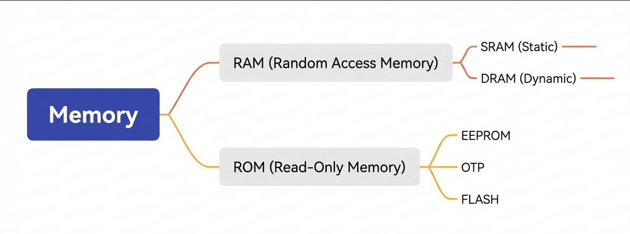
RAM (Random Access Memory)
Random Access Memory is the internal memory used for direct data exchange with the CPU. It allows for high-speed reading and writing (except during refresh cycles) and typically serves as a temporary storage medium for the operating system and active programs.
Key Characteristic: Once power is lost, the stored data is lost (Volatile Memory).
SRAM (Static Random-Access Memory)
Static Random-Access Memory is a subtype of RAM. The term “Static” implies that data is retained as long as power is supplied, without the need for refreshing.
Due to lower integration density compared to DRAM, SRAM is generally utilized for high-speed caches (Level 2 Cache) in microcontrollers.
DRAM (Dynamic Random Access Memory)
Dynamic Random Access Memory is another subtype of RAM. “Dynamic” indicates that the stored data must be periodically refreshed to be retained.
DRAM has a higher integration density than SRAM and is commonly found in standard computer memory modules (RAM sticks).
ROM (Read-Only Memory)
Read-Only Memory stores fixed information. In normal operation, data can only be read and cannot be instantly modified or rewritten.
The primary advantage of ROM is its non-volatility (data retention without power).
EEPROM (Electrically Erasable Programmable Read-Only Memory)
EEPROM is a modifiable ROM that can be erased and rewritten by applying a voltage higher than the standard operating voltage.
It is frequently used to store hardware configuration data, such as a PC’s BIOS or non-volatile parameters in embedded devices.
OTP (One Time Programmable)
Data written to OTP memory cannot be changed or cleared.
Commonly used for writing permanent product IDs and security keys.
FLASH Memory
Flash is a block-erasable non-volatile memory. Unlike RAM, Flash retains data without power, yet it is rewritable. At low voltages, it acts like ROM (read-only), while at higher voltages, it allows modification similar to RAM.
- In MCU applications (like the APM32), Flash is primarily used to store program code (Firmware).
- Note: Flash erase operations are performed in “Blocks.” Engineers must pay attention to byte and address alignment during programming operations.
02. CORTEX-M4 MEMORY MAP ARCHITECTURE
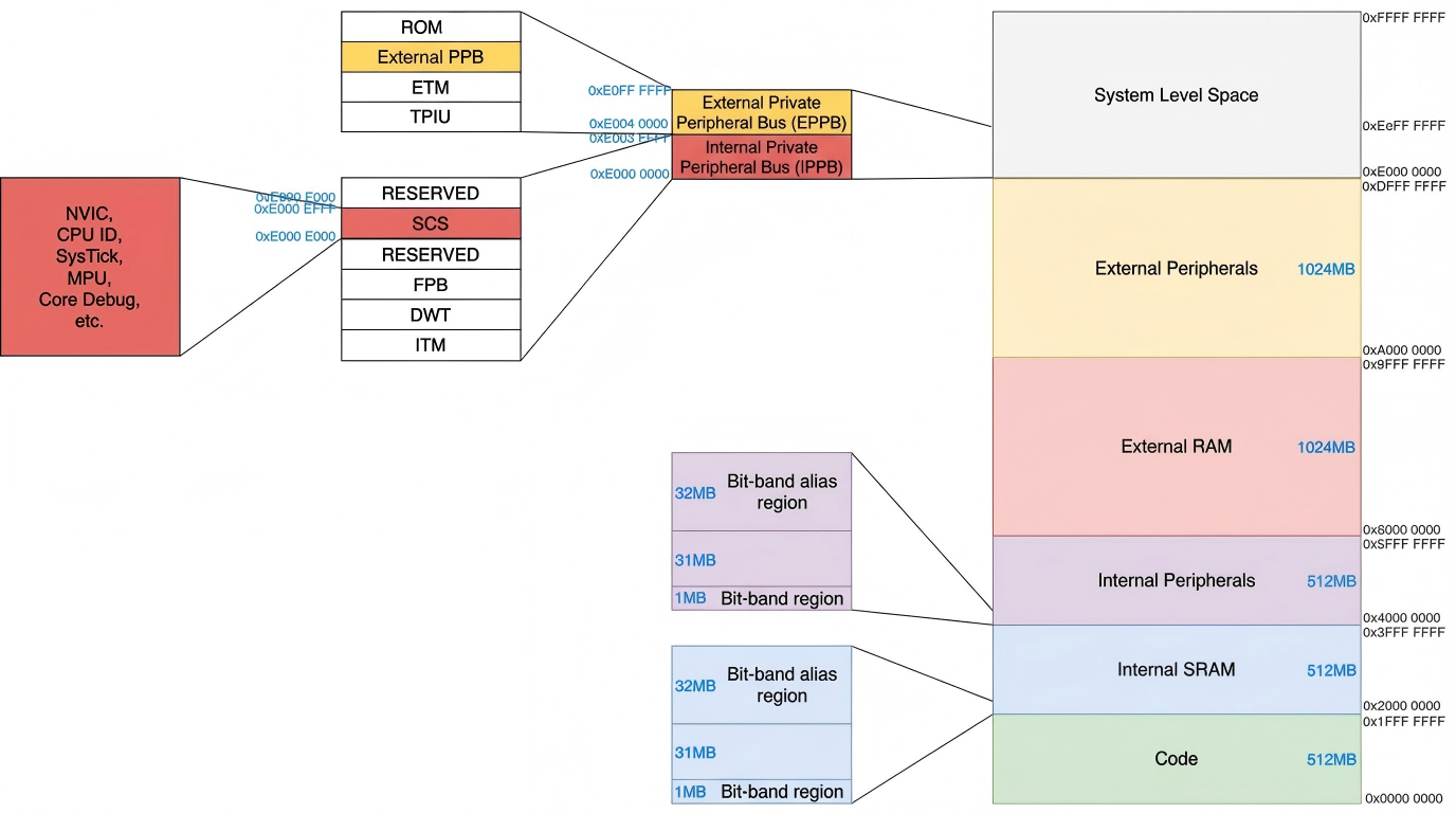
The Cortex-M4 core utilized by the APM32 relies on FLASH and SRAM, and may interface with off-chip DRAM. The Cortex-M4 provides a linear 4GB addressable space, segmented into:
- Code Space
- On-chip SRAM
- On-chip Peripherals
- Off-chip RAM
- Off-chip Peripherals
- System-level Space
The System-level space houses the NVIC, SysTick, and MPU. Additionally, a 2MB “Bit-band region” exists within the on-chip SRAM and peripheral spaces to support atomic bit-band operations.
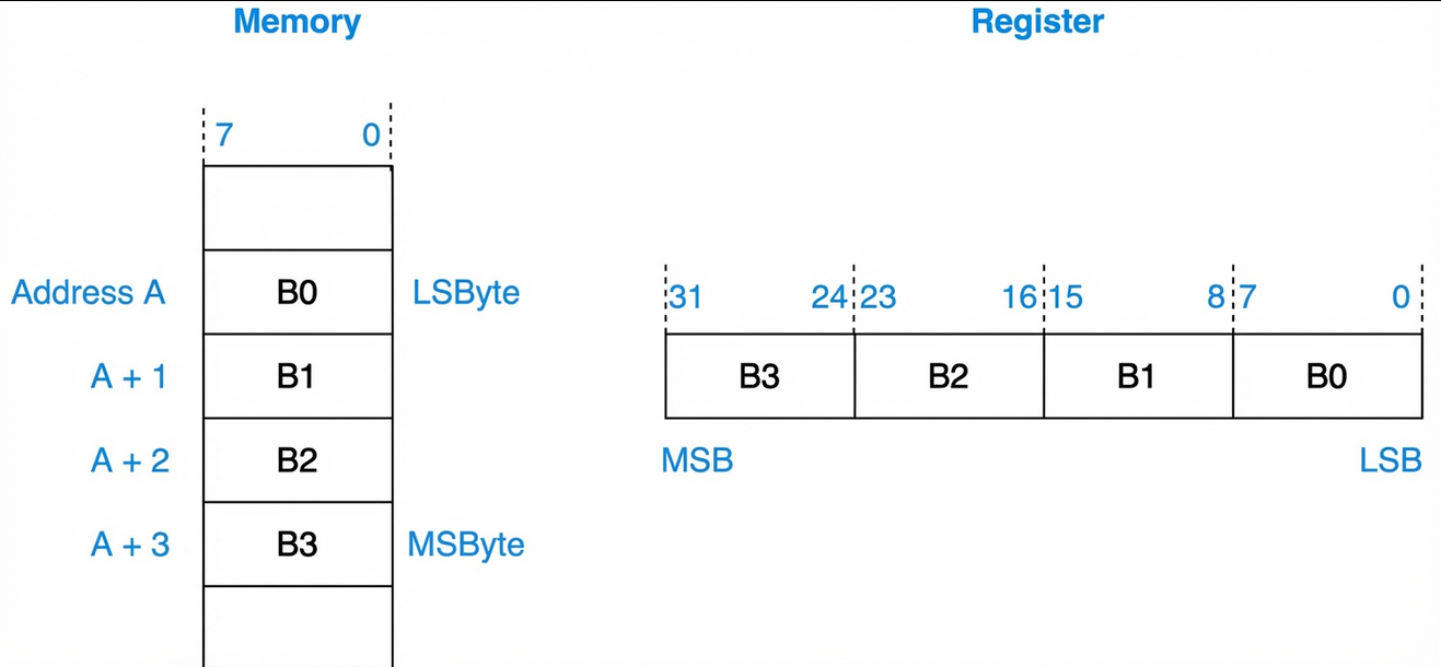
The Cortex-M4 core supports both Little-Endian and Big-Endian modes but defaults to Little-Endian, where the Least Significant Bit (LSB) is at the lower address.
Best Practice: Design buses, peripherals, and data structures using Little-Endian mode to ensure compatibility.
03. APM32F407 MEMORY MAPPING AND ARCHITECTURE
Let’s analyze the specific architecture and memory composition of the APM32F407xx series.
System Bus Architecture
Before examining the map, understand the data flow. The master bus connects to the slave bus via a Bus Matrix. For instance, when data moves from SRAM to the DMA1 peripheral, the Bus Matrix arbitrates the transfer to DMA1 via the AHB1 bus.
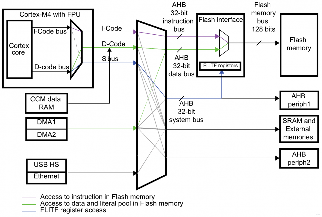
Core Concept: Data interaction between memory and peripherals is facilitated entirely through the bus system.
APM32 Memory Composition
The APM32F407xx series integrates:
- On-chip SRAM
- On-chip Flash
Understanding Memory Mapping
What is memory mapping? Since physical memory lacks intrinsic address information, the CPU requires a distinct identifier to locate storage units. This identifier is the address code.
In the APM32, different memory types are treated as blocks. Each block is assigned a continuous set of hexadecimal numbers representing addresses. The association of these addresses with physical memory blocks is defined as Memory Mapping.
Simply put: Assigning the chip’s theoretical address space to physical storage hardware is memory mapping.
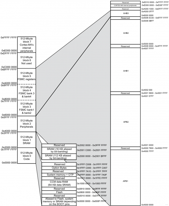
SRAM Configuration in APM32
The APM32F407xx series features up to 196KB of SRAM, comprising:
- 4KB Backup SRAM (Battery Backup Domain)
- 192KB System SRAM
System SRAM supports byte, half-word (16-bit), and full-word (32-bit) access at full CPU speed (0 wait states). It is divided into:
- 112KB + 16KB Blocks: Mapped at
0x2000 0000 to 0x2001 FFFF, accessible by all AHB masters.
- 64KB Block: Mapped at
0x1000 0000 to 0x1000 FFFF, accessible only by the CPU.
Flash Memory Configuration
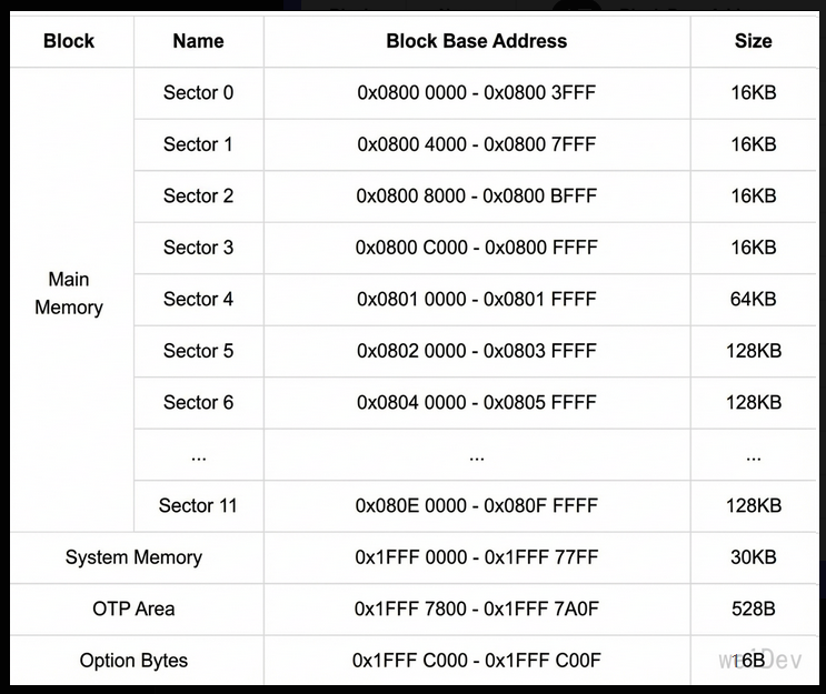
The APM32F407xx offers up to 1MB of Flash, supporting 128-bit wide reads and various write widths.
Flash Structure Details:
- Main Memory: 4× 16KB sectors, 1× 64KB sector, and 7× 128KB sectors.
- System Memory: 30KB for the system bootloader.
- OTP Memory: 512 bytes for one-time user data (plus lock bytes).
- Option Bytes: For configuring read/write protection, BOR, and watchdog settings.
Memory Remapping and Boot Modes
Typically, the MCU boots from 0x0000 0000. To support booting from different media (Flash, SRAM), Memory Remapping assigns these media to the boot address.
Booting is often referred to as “Bootstrapping” in embedded engineering.
By configuring the BOOT[1:0] pins or the SYSCFG_MMSEL register, you can:
- Run the System Bootloader (ISP).
- Debug code in RAM for speed before flashing.
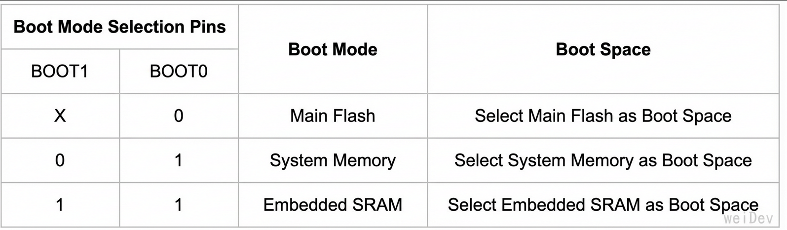
Note: The APM32 code region starts at 0x0000 0000 and the data region at 0x2000 0000.
04. APM32 REGISTER MAPPING GUIDE
What is Register Mapping?
In the APM32F407xx, peripherals reside in the address range 0x4000 0000 - 0xA000 0FFF. Accessing peripherals via raw 32-bit addresses is error-prone.
Register Mapping is the process of assigning human-readable aliases (names) to these specific memory addresses based on their function.
Below is a practical C code example for mapping the GPIOC Data Output Register.
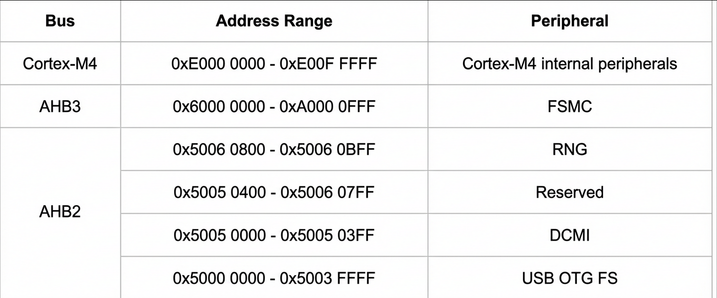
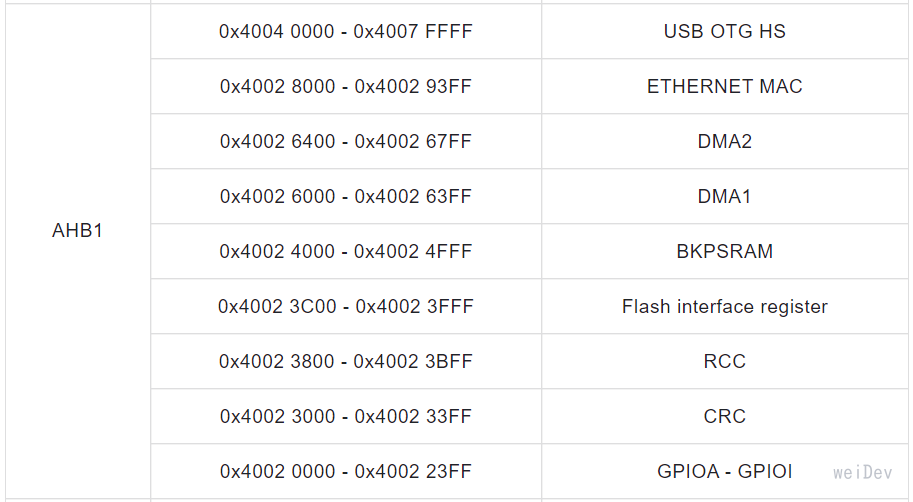
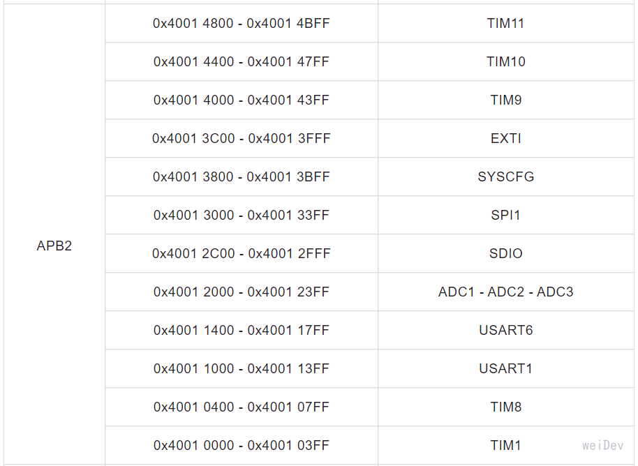
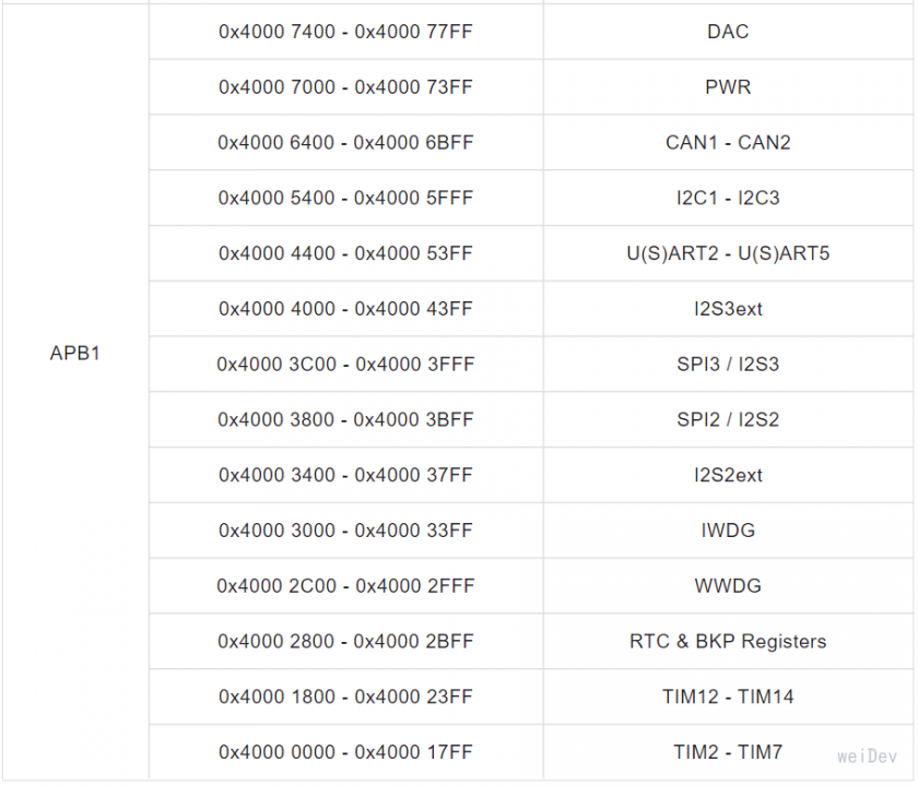
According to the datasheet, GPIOC is connected to the AHB1 bus.
/* Peripheral Base Address Definition */
#define PERIPH_BASE ((uint32_t)0x40000000)
/* Bus Address Calculation */
#define AHB1PERIPH_BASE (PERIPH_BASE + 0x00020000)
/* GPIOC Base Address */
#define GPIOC_BASE (AHB1PERIPH_BASE + 0x0800)
/* Type Casting to Structure */
#define GPIOC ((GPIO_T *) GPIOC_BASE)
/* GPIO Register Structure Definition */
typedef struct
{
union
{
__IOM uint32_t MODE; /*!< Address offset: 0x00 - Mode Register */
struct { ... } MODE_B;
};
/* ... (Other registers omitted for brevity) ... */
union
{
__IO uint32_t ODATA; /*!< Address offset: 0x14 - Output Data Register */
struct
{
__IO uint32_t ODATA0 : 1;
/* ... individual bits ... */
__IO uint32_t RESERVED : 16;
} ODATA_B;
};
} GPIO_T;
/* Example: Setting Pin 0 of GPIOC to Low */
GPIOC->ODATA_B.ODATA0 = 0;
Important: Always remember that the Cortex-M4 architecture defaults to Little-Endian mode when manipulating registers.